Competencies
For our system solutions we combine high performance software with ultra-precision hardware
With our well-educated team of engineers and technicians, we develop all key system functions in house, such as mechanical and electrical design as well as the programming of the production flow.
Our customers work with modern technology on future applications including automotive, medical, opto electonics and micro electronics. Space technology, data and telecommunication as well as semiconductor industry are further key industry sectors.
In all of these companies, new production technologies ensure a competitive edge. In addition, the ongoing miniaturization of the devices asks for innovative processes.
Our customers successfully use the nanosystec production solutions to cope with these challenges.
Our promise: Precision and reliability
nanosystec stations combine precision and reliability for industrial manufacturing processes.
Our added value promise comprises:
Quality Management
Since July 2014, nanosystec has been certified according to ISO 9001:2015 (9001:2008). We continuously improve our quality to ensure a safe fundament for the successful collaboration in challenging technology projects. We will be happy to provide more information on this topic for interested parties.
Highest precision
We precisely position and assemble devices down to 0.2 mm size with a precision of < 100 nm.
Maximum process reliability
Our solutions guarantee maximum reliability in industrial production.
Individual solutions
We look for challenging requirements! Finding new solutions is one of our strengths.
>20 Years process experience
Interdisciplinary experience is valuable. We offer this treasure for your application.
Made in Germany – used all over the world
Whether in Europe, North America or Asia: we support you with our international network.
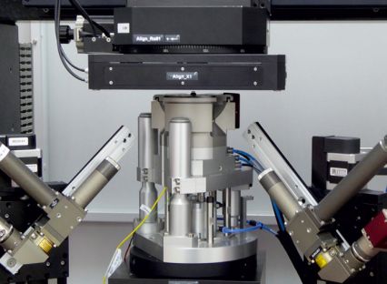
Active Alignment with OptoSpin
The coupling of fiber and fiber arrays to chips and modulators is a critical task. Conventional coupling delivers high quality results but the time needed for active alignment is often too long. OptoSpin overcomes this hurdle.
The feedback signal drives the motion stages of OptoSpin. With a response time in the order of microseconds, it takes less than 1 second to reach the optimal position in most of the cases. Compared with passive placement, OptoSpin is nearly as fast and the resulting losses are much smaller.
OptoSpin is an option for all nanosystec systems with active alignment. The nature of optical coupling with laser, fiber and fiber arrays, chips and modulators and similar devices is well suited for efficient use of OptoSpin. But this is not the limit – every application which needs positional correction as a function of an electrical signal benefits from this technology.
Ideally, the fast alignment engine is part of a Nanosystec system from the beginning. But also a later upgrade with OptoSpin is a viable possibility.
OptoSpin is designed for high speed. The moving masses are small and the driving forces high. Capacity sensors serve for position readout and the resolution is in the order of a few nm. Despite its ultrafast speed Optospin carries relatively high loads without deteriorating its performance.
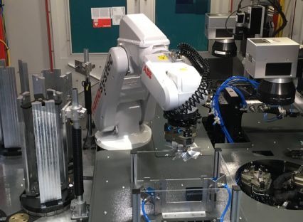
Automation
Automation offers several key advantages for manufacturing processes. The product quality is consistent from piece to piece. Machinery is better utilized as the systems works 24/7 while manual labor is reduced to a minimum. In this way, efficient production is also possible in production lines where labor cost is high. In addition, ramping of the production volume is easily achieved by adding identical stations – without the need of long training periods.
Nanosystec stations combine automated part handling with the micro assembly of optical elements and other miniature components. The stations utilize either active alignment or passive placement processes. Joining methods include epoxy gluing, laser micro welding, selective laser soldering and fine cutting.
In many manufacturing environments, the production for a new product starts with a single set-up and process definition. The nanosystec production stations fulfill this requirement and provide an upgrade path for future automation.
Loading the components to be assembled on a device tray is one approach. These trays are then loaded into the system with conveyor belts. An alternative method are feeders, e. g. with standard dimensions like Jedec trays. Each feeder carries up to 20 of these trays and the finished product is loaded back onto receiving trays. If devices are already available in trays, a robot can pick the components and bring them into the working position.
When working with mixed processes and/or components on the same machine, identification tags on the trays call relevant parameters and processes. No human intervention is needed and all manufacturing steps are executed automatically.
Depending on the material flow and the desired production volume, nanosystec will propose a tailored solution for the respective application.
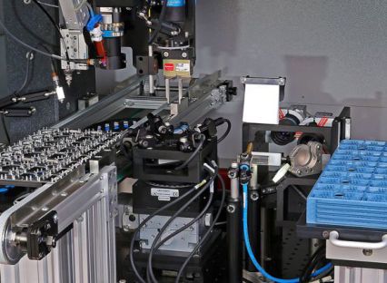
Cartridge Concepts
The devices will be placed into a cartridge or device tray. These cartridges use a generic machine interface in the nanosystec workstation. Depending on the manufacturing process, the cartridge may contain one or several sets of components.
The loading procedure of the cartridges takes place outside of the system in order to minimize the core process time. With two or more cartridges, the system achieves optimum utilization even for manual laoding. Also different device types are easily accomodated as the machine interface remains unchanged.
The cartridge concept is an elegant way to handle optical components with fiber pigtail. As the fibers can be coiled and being protected, there is less risk of damage.
When further automation is required, stop motion conveyor belt leads to full automation of the production process. The nanosystec workstation is then seamlessly integrated into a production chain.
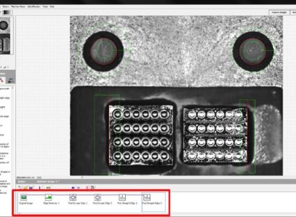
Machine Vision
High-performance machine vision is the base for repeatable, automated processes. The illumination of the objects needs to be combined with adapted routines for a reliable recognition.
In the nanosystec stations, the intensity of the illumination in various colors can be adjusted as required. The synchronization with the camera picture allows for a fast recording. For the image recognition, often several routines will be combined, such as edge detection and pattern recognition. Critical pictures will be stored during the processes for further optimization of the algorithms.
In order to shorten the process time and increase the reliability, the pictures of various cameras will be combined. Depending on the application, telecentric and zoom lenses will be used.

Metrology
The diminutiveness of the parts and the request for forceless measurement favor non-contact or low-force methods.
The assembly and alignment of electro optical components require the precise measurement of distances with a resolution and precision in the sub micrometer range.
The standard method is the camera system itself which is basically implemented in every nanosystec workstation. Machine vision algorithms including autofocus determine distances and orientation of the parts for gripping and prealignment. A calibrated motorized zoom allows for working in different fields of magnification.
Confocal sensors deliver results with a precision of a fraction of a micrometer. They are fast, compact and have a small measurement spot. This is of advantage if the object to be measured has fine structures and features.
If the objects can accept a small force, tactile sensors generate fast and precise results. They fit in almost every setup. Alternatively, strain gage assemblies determine the contact surface between the parts.
Multiple Beam Optics
In order to create a weld or solder joint, various approaches can be used.
The most versatile but low volume method is the single point attachment. Either the focusing optics or the device are moved perpendicular to the incident beam to reach the respective position.
This method is well suited for process development and feasibility.
For the welding joint, large energy and a short time interval of several milliseconds are required. Therefore, XY scanners offer a possibility to deviate the beam fast from one position to the other. A working area of 50 mm to 1mm edge length can be realized.
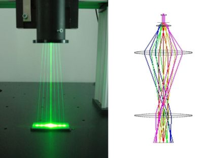
Multiple Beam Optics are of advantage when various spots have to be repeatedly set in a fixed geometry. This method avoids tombstone effects in welding or soldering joints. This happens for a single beam, when one side of the component is attached and starts tilting.
For soldering procedures, the process times can be cut tremendously. The soldering takes at least a second to melt the solder material evenly and the power level is substantially lower compared to welding. This means that the beam can be split into various spots.
The Multi Beam Optics used by nanosystec split the beam into various spots which can have different energy distribution in order to adapt it perfectly to the requirements of the device. This method ist the superior choice for high-volume selective laser soldering.
Precision Mechanics
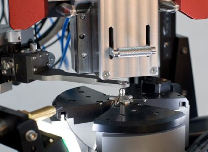
High-precision mechanics allow micro attachment procedures in the sub micrometer regime.Our stations are equipped with industrial grade motion systems of best mechanical accuracy.
Crossed-roller bearings cope with high loads and provide ultralow runout.
The motion assemblies are built onto stiff granite structures. These provide a large inertia and therefore are ideally suited to accomodate fast moving stages while keeping stable.
The ultra-precise machining of removable system components provides defined positions within the automated processes. This leads to high passive positioning accuracy and reduces process times when applying active alignment procedures.
nanosystec uses commercially available high-precision solutions whenever possible. Device specific toolings, such as grippers and cartridges, will be produced by a network of qualified suppliers. These provide modern machining technologies, such as wire-cut EDM, spherical polishing and grinding as well as specific surface coatings.
Process Software
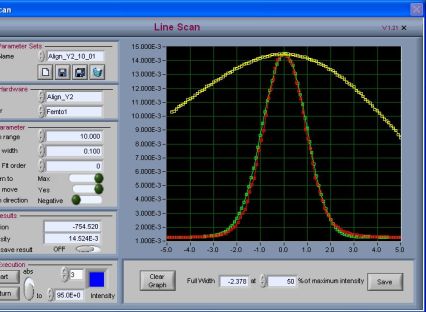
The TestMaster process software is a versatile process development and production tool. It combines a large number of functions and devices which can interact with the system directly or via a sequence editor to run fully automated processes.
Various user levels allow to limit access to all of the functions. The permissions can be individually configured.
Customers have full access to the process programming in order to optimize process procedures and adapt them to changing requirements.
Powerful machine vision tools allow full process automation including pattern recognition, autofocus, etc.
Alignment algorithms run whenever possible directly in the motion controller in order to cut process times to a minimum. These include spiral searches, up to 5 axes optimization routines and many more.
Customized modules can be integrated on request.
We support your entire process of product development:
From concept via prototype to serial production
Assistance in early stages – e. g. with feasibility studies
Individual, tailored and customized production solutions
We will work with you on new processes to be automated
Send us a message
Call back
Request information
Send us a message
Call back
Request information

